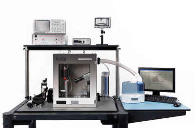
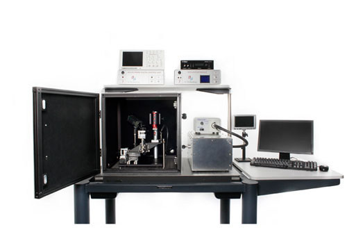
The standard Relative Humidity Chamber creates a local, 80 litre, environment whereby the Relative Humidity (RH) can be adjusted within 1% and we have an optional sample heater working from Room Temperature to 90˚C, both can be automatically controlled.
The RHC can also act as a light enclosure with light source either integral or piped in via semi flexible fibre optic tube. The light sources can be optionally controlled in terms of intensity and wavelength for Surface Photovoltage Spectroscopy. We have both DC and AC SPV modes.
For metals the RHC would be used to measure the corrosion potential (changes in electrochemical potential) under standard condition.
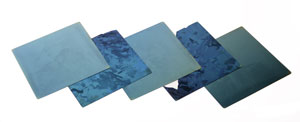
[For example measuring specific metal samples versus varying RH levels both on cleaned surfaces and surfaces covered with a thin chemical layer.]
For some insulating surfaces (or dielectric) RH control is necessary to dissipate surface charge.
For some solar cells the surface and interface trapping constants are very sensitive to cell temperature, i.e. Voc and solar cell fill factor is affected. For some organic semiconductors control of RH during measurement is required. We have also encountered other forensic projects where RH control is required.
Lastly the chambers are sufficiently large (and the bottom is an optical table with mounting holes) to permit mounting of other equipment and easy mounting/dismounting of samples.
2.(i) What is the surface Photovoltage option for and how is it different from your Base, System & Scanning Packages?
We offer several forms of SPV, essentially they are the same across our product range, however the physical implementation may differ, for example in Ambient and Ultra High Vacuum environments. Firstly there is the simple programmed DC-SPV (SPV010) of a light source being switched on and off, synchronised with surface potential (SP) measurements to produce delta (SPV) = SP (Illuminated) -SP(Dark). One can also manually switch the light source on and off and watch the SP transient (approx 1000 measurements/min). Most devices have decay times in the seconds to minutes range. Results over longer periods are not well known as probably the only way of measuring the SP on longer timeshares is with the Kelvin probe.
The light source can be either high intensity LEDs (which work very well) or QTH lamp. The QTH lamp is useful both by itself and for a source of wavelength specific SPS.
The next SPV system SPV020 is of most interest to general customers, in this case all the features of SPV010 apply but in addition the light source intensity is controllable, thus a plot of SPV versus light flux is produced. This can be useful for scoping out the whole response: in the cells I have measured to date both Voc is variable (say from 250 to 450 mV) as is the light sensitivity curve. There is certainly interesting data there and if the light source output was independently calibrated perhaps a rough guide to Air Mass would result.
We can offer the above systems with or without a light enclosure, secondly we can offer a variant of SPV020 with an optical chopper resulting in AC-SPV.
Lastly we offer either motorised linear variable filter (SPS030) or motorised monochromator (SPS040) systems to probe the specific wavelength dependency of SPV from 400-700 and 400-800 nm respectively. The LVF produces perhaps a higher light intensity than the monochromator system, however the pass band is obviously somewhat larger. We can optionally additionally populate the system with infra-red LEDS to cover higher wavelengths than can be easily obtained with either filter or monochromator system.
The base, system and SKP packages do not offer automatic SPV however obviously one can implement one's own light source and switch it on and off to measure SP. Having used both ways in the past we know that it is much more efficient researching photosensitive behaviour with SPV/SPS using the automated systems. It allows the possibility to specify the experimental protocol so that a non-specialist can undertake the measurements and they will be comparable.
2.(ii) What do people use your different SPVs for?
Customers use the SPV for solar cell research, organic and traditional semiconductors, "new” semiconductor characterisation, dye sensitive films, etc.
3. Your literature states that you also supply the scanning platform with the SKP5050. Does that mean the regular SKP system does not have the scanning platform?
While the SKP does include a scanning stage, the SKP5050 is outfitted with what we believe is necessary to have a useful measurement tool. Before this product was introduced customers buying the SKP would tend to opt for all the additional features now contained in the SKP5050 system. Customer feedback indicates they are well used.
This is our best selling Kelvin probe system has been since it was introduced.
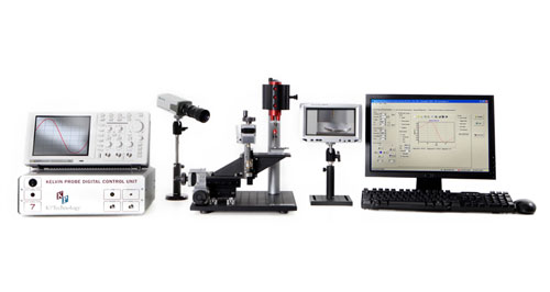
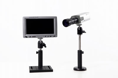
4. You write that with your SKP5050 package you supply the optical/TFT monitor arrangement to monitor tip-to-sample displacement and tip positioning on the sample. How are these functions achieved in other, not SKP5050 packages?
The TFT monitor/camera arrangement can be configured to watch the probe position on the sample or in higher magnification the separation of the tip and sample. On some surfaces this can be difficult to see by eye. Also with our smaller tips, e.g. 50 microns diameter, camera positioning is necessary. Note that this is used for initial tip position and as a general visual check to see where the tip is currently on the sample, for instance on several of our in-house systems the PC is separate for the optical table or desktop supporting the KP/SKP/RHC-KP.
After initial macro-positioning beside the equipment reverting to computer control of tip to sample spacing is far more accurate. There is an option to keep sample to tip spacing constant to within 1 micron during scanning and this is done by monitoring the Kelvin probe signal and automatically adjusting the sample height to the vibrating tip.
In non-motorised system it is possible to use a DC Offset applied to the voice coil. However the motorised systems give 25 mm of height control and the DC Offset only about 0.1 - 0.3 mm.
5. You write that your System Package has tip positioning of 25.4mm. What does that mean? Is the tip that high over the sample?
The sample can be moved vertically 25 mm with respect to the tip. As samples are mostly quite flat, during a scan, only a short range is used.
The sample can be retracted for sample changing or the tip can be manually retracted 25mm too. Both the manual and motorised translators mean that, with minimum fuss a range of sample sizes can be accommodated.
6. If in KP010 and KP020 the tip is 2mm, does that mean that the lateral resolution is also 2mm? Or is it the length of the tip and why is this important?
We estimate that a 2mm tip provides sufficient spatial resolution for most of our users to get started. However we also offer a 50 micron tip and in this case the scan size is typical 500-3000 microns per side. Please view the attached Probe Resolution PDF with some examples of large and small scans.
The Kelvin method is a capacitive method and thus the probe averages the WF underneath the tip. The spatial resolution is essentially the probe diameter. Newton’s fringing field terms do apply (to broaden the effective area) however in general this is not an issue with macroscopic tips. Professor Baikie has achieved 2 micron resolution and on binary systems (2 work function involved) has applied 2D deconvolution to determine the precise location of an interface with 1/20th of the tip diameter. Though he does not claim to be able to do both at once!
Higher spatial resolution is feasible however as we are approaching the limits of the measurement environment and operator capabilities, we have elected to supply 2 mm tips as standard and 50 micron tips for anyone who wants higher resolution. We also offer an in-line tip holder that allows the client to screw in any diameter tip they require. We use this system form our larger SPV tips: 5, 10 and 20 mm diameter (semi-transparent).
In summary the tip diameter is the lateral spatial resolution, the length of the tip is not so important, obviously if it is too long then the tip may oscillate in the lateral direction and this would degrade resolution.
7. Does KP010 require that a customer has their own sample mounts?
Yes, this option is included in our range (in a similar fashion to the SKP010) as a "catch-all" for those customers that specifically want to control their own sample. However KP020 and SKP5050 remain, by far, the most popular Kelvin probe configurations that our clients order. We do not recommend a KP010 configuration to any but the most experienced user, there are too many things that a novice user can get wrong or misinterpret the importance of and frustration will result. Our configurations mean that one can get started straight out of the box.
8. In what situation is the Faraday cage most useful during the KP measurements?
The simple faraday cage we supply will shield the equipment from electric fields due to the operator (the chair the chair they are sitting on), equipment on the desk and in the vicinity. Note an operator can be at a static potential of 2000-3000V after arising form a plastic chair. If the first thing they contact is the faraday cage there is no problem however if the touch a dielectric sample they can charge it up, also if they touch the tip amplifier they can damage it.
Moving up a scale the optical or RH enclosure keeps sample dust free, their mass tends to minimise mechanical disturbances (from the environment) and isolate the experiment from scientists (and visitors) passing through a lab generating air currents and noise. If one works in a quiet corner with a skilled operator then the faraday cage may be consider redundant, however in a general purpose busy laboratory then either a simple screen or better still an enclosure is well worth employing.
9. What are the lateral resolutions of KP010, KP020, SKP010 and SKP5050?
The lateral resolution of all these system is the tip size we employ. We have 2mm as standard, 50 micron as an option (really only for SKP) and we have an alternative design termed the ‘in-line’ tip that covers all suitable diameters (using a stainless steel tip). This is a feature that has evolved through the years with customer suggestions and demands. For a 2mm tip the lateral resolution is 2mm.
10. You write that the SKP010 has three motorised axes X,Y & Z. What is the Z axis for?
X,Y is the sample plane (i.e. scanning axis) where Z controls the tip to sample spacing. In a scan this is required if the sample is not perfectly flat or has not been mounted perfectly flat.
11. Does the SKP5050 have all the software features of SKP010?
Yes the SKP5050 has all the features of the SKP. The SKP5050 is equipped with all the add-ons we feel are necessary to make it an excellent all round measuring tool.
12. What is the main advantage of having SKP5050 over SKP010?
SKP5050 has all the features of the SKP plus all the add-ons we feel are necessary to make it an excellent all round measuring tool.
13. Does the GBC030 require a connection to a Nitrogen tank?
Really this is up to the operator. Although N2 is the most widely used blanket gas we have designed gas cells for clients who intended to use alternatives. The outlet of their gas sources were directly connected to the chamber. So we can terminate the gas line in any fashion required by the client.
14. Can you use KP010, KP020, SKP010 or SKP5050 in a glove box?
Yes indeed. These systems have been used in glove boxes around the world and this was the reason we introduced our own range of solutions based on the GBC030.
15. In SKP250250 what is the third translating dimension (50mm) for?
In this system we use larger translation stages than the SKP5050. We intend to, later in the year, incorporate an automatic calibration system. To accommodate this upgrade we have elected to make this (Z) stage 50mm. At the moment the client has to mount the reference sample, then dismount and mount the sample. The upgrade will remove these additional steps.
16. For how long do Gold Coated Reference Samples usually last?
Discerning customers tend to come back for new gold samples after they have been badly treated; 6-18 months is realistic. Gold coated tips have to be held pristine and after a major sample to tip contact they can no longer be considered ‘gold covered’. We feel the gold reference sample is absolutely necessary in a Kelvin probe setup.
17. I was under the impression that work function should be measured in eV or meV but I have read literature stating work function resolution of 1-3mV. Is it right?
In physics, for charged particles (such as electrons) the formula E= eV applies where E is energy, 'e' is the charge on an electron and V is volts (or millivolts).
The work function is the energy required to remove an electron from the surface of a conductor such as a metal. It is an energy and the units are typically 'eV' or alternatively 'meV'.
The Kelvin probe actually measures a change in voltage either in volts or millivolts; sometimes this is called a surface potential change. So the difference between work function changes (measured in eV) and surface potential changes (measured in volts) is simply the charge on the electron 'e'. Most scientists and engineers recognise this and use the two terms independently.
You could take the following view: The Kelvin probe reports surface potential changes in 'mV', calibrating the tip work function and converting the measured voltage value to a sample work function allows you to quote in 'eV'.
In summary, whilst technically correct, the work function resolution should be stated as 1-3 meV.
In addition the work function resolution is a function of the tip size. So for a larger tip (1-2 cm diameter) we will have 0.1 meV resolution. As our new Kelvin probe tip holder (which is an option) allows us to use any tip diameter then in our new literature we are quoting a work function resolution from 0.1 meV, or indeed 100 µeV.
18. We are testing your SKP instrument to measure the potential on a sample surface. The potential (work function) is a relative, not absolute, value. What is the reference?
It is correct that the Kelvin method is a relative one, however if the tip is calibrated against another 'reference' surface then the tip work function is known too. However this value is obviously only as good as the value taken for the reference surface.
Our ambient KP Technology Kelvin probe systems are shipped with a 'reference' sample composed of two metals, Aluminium (Al) and Gold (Au). The objective of this sample is for you to measure on the gold surface, and taking the gold reference as 5.10 eV absolute, calculate the tip work function. The objective of the Al
surface is as the work function of Al is about 1V less than Au, measurement on this surface tells you whether the tip is below or above Au (5.10eV). Our experience is that the tip is between 50 and 200 mV below gold. The range depends upon tip handling during mounting and tip treatment in operation (i.e. history of tip to sample collisions).
For instance if the tip to gold contact potential difference (CPD) is 200 mV and the tip to aluminium CPD is -800 mV then the tip work function is 200 mV below gold, i.e. approximately 4.90 eV. The Aluminium work function is then 4.90 - 0.80 eV, i.e. approximately 4.10 eV. The stated value for Aluminium of about 4.2 - 4.3 eV and the reason your Al surface is initially lower is that we mirror polish the Al, the surface changes and the polishing media tend to lower the bare Al surface work function slightly.
You will probably find that the Al surface slowly oxidises (over a period of months and years). This will cause the mirror finish to become tarnished and the work function to rise to 4.5 - 4.6 eV. However the gold surface, if held pristine, will maintain its work function. One must remember when using gold in this way that it is sensitive to humidity and if the humidity in your laboratory changes the measured CPD will too, however generally these changes are quite small 10-30 mV for the typical humidity changes in a laboratory, some of which are climate controlled in any case. When using the reference sample one must also remember that the gold surface is fragile and can be damaged by tip contact, fingerprints etc. We recommend that you consider changing the reference sample every 3-6 month (depending upon its use and condition). It cannot be mechanically or ultrasonically cleaned without damaging the gold. Note - It should be possible to extend the life of your sample with careful handling and storage in a separate enclosed box.
Replacement reference samples can be purchased from the KP Technology online store. Click here.
If you find that the data you get for your reference sample on gold is -200 mV and for Al is +800 mV then there are two possibilities (i) you have applied the backing potential to the sample rather than the tip, or (ii) you have changed the trigger position of the incoming waveform so that it now triggers at a
point 180 degrees advanced in time than when we set the default parameter. Both of these operations would result in the CPD data being multiplied by -1, neither will however change the magnitude of the CPD.
Here is another important point to consider. As a PhD student Prof. Baikie found that the CPD between two surfaces changes with probe parameter (amplitude of oscillation, mean spacing between tip and sample, Vb applied to tip or sample). These results are published in both his thesis and in the journal "Review of Scientific Instruments". They showed the importance of using exactly the same set-up to compare CPD measurements on Al, Au and other samples. In his system this involved keeping the gradient approximately constant (for example 300 with an allowed error of 20). If you do not maintain this consistency (either manually or automatically and using the same parameter file) then, in general, the CPD data will differ each time you take a new measurement. It is this property of accurate, repeatable data, that distinguishes KP Technology equipment from other vendors.
19. When exposing our sample to a high RH we find a water layer would form on the surface.
We want to know the maximum thickness of the water layer that your instrument can normally work. 0.2 mm, 0.5 mm or 1.0 mm?
This is something we have experienced on occasion with our in house sample analysis. So far we have not reached a limit on the water layer thickness, and certainly not in the range you mention. Provided the liquid conducts you will be sensitive to the topmost layers.
In earlier experiments of polar liquids (where we scanned across the liquid surface above the gold - aluminium interface). We found that for some liquids the interface (with 1V built-in surface work function change) was invisible, in other cases the interface was still visible but the potential changes was reduced. In these cases the liquid layer was not less than 2mm thick.
Never-the-less the liquid build up still has some practical implications:
1. If evaporation occurs this may destabilise the liquid surface level.
Use of our dedicated relative humidity chamber makes this less of an issue.
2. If you pre-treat the surface to reduce surface tension then the water may flow.
You may wish to consider making a trough or reservoir in a sample to accommodate the fluid.
In order to determine the water thickness we suggest that you first make a measurement (at gradient 300) on the bare surface and note the Z motor displacement. Then back the probe away automatically, add the salt solution and re-insert the probe towards the liquid surface. If you now record the Z displacement at gradient 300 you know the liquid layer thickness.
If you are using the SKP for these measurements a lot, it may be worth considering an upgrade to a larger diameter tip and our new in-line tip. We can accommodate any diameters (though most commonly 0.05 to 20 mm). We can also make the tip with holes in it to allows air penetration. The larger tips will result in a larger stand-off height and thus minimal disruption to the liquid surface.
20. I am interested in using Kelvin probes to determine information about the grain and grain boundary characteristics (i.e. effective work function due to traps, trap energy and density) of our thin film samples. As I am not familiar with the technology, could you provide some information regarding the application of Kelvin Probes for polycrystalline thin film characterisation.
Our in house research has give us the opportunity to work with Polycrystalline Si thin film for a number of years. The key point for us was understanding that the long term decay states at the dielectric interfaces played an important role in determining Voc and thus the fill factor and energy extraction. A surprising aside was to discover how the cells responded (detrimentally) to temperature change and for this point we have been very careful in interpretation claimed specifications determined at 20°C as in strong sunlight the surface temperature of the cell can be considerably higher and cell efficiency actually starts to degrade.
From the beginning of our research we were aware of SPV mapping on semiconductors using pulsed light through a semitransparent electrode. The objective of this experimentation was to determine chemical contamination of crystalline Si wafer via changes in de-trapping lifetime and involved high speed data acquisition (>1MHz). However such system simply cannot measure slow states (this is clearly the domain of the Kelvin Probe), e.g. at a speed of 1000 measurements per minute (referred to as DC-SPV), and it is within these slow states that much of the effect of Voc is determined. These SPV transients are easy to record and product surface potential changes of between 250 and 450 mV (depending on semiconductor and cell structure) make them easy to measure.
Our recent experiences have been with a series of solar cells and dye sensitive films. Our work has resulted in the commercial release of our Surface Photovoltage Spectroscopy equipment based upon a motorised Linear Variable Filter (high intensity, 400-700nm, broad pass band) and a motorised monochromator (low intensity, 400-800nm, narrow pass band). We currently use the SPS equipment in both DC-SPV and AC-SPV modes.
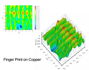
We have used a 50 micron diameter tip in our SKP5050 system to seek obvious macroscopic (optical) grain boundaries in oxide and nitride coated mc-Si and have recorded approx 70mV surface potential changes across the grain boundaries. Further SEM/X-ray Crystallographic studies of micro-crystalline metal alloy surface indicate a complex grain boundary structure and although we have not yet found a way to resolve these surface potential changes laterally, the Kelvin Probe, electrically, via charge trapping and de-trapping is another matter. There is a high probability that charge trapping and release can be observed, however it would involve a separate technique to establish a relationship between electrical and physical/chemical characteristics.
To summarise, with reference to your specific queries: we have evidence that the effective work function is affected by grain boundaries and this is backed by the order of magnitude surface potential changes one would anticipate from Miller index variations. However dielectric or oxide coatings may tend to mask these changes and the spatial (lateral) resolution may not be adequate. Changes in effective work function due to light stimulated trapping and detrapping are another matter and we do recommend this as a strong possibility for future study, however other techniques/data will be required to correlate with the WF/SP changes observed.
21. The application I am working with requires a very specific lighting configuration with control of wavelength and interference filters. Can your system accommodate this?
We currently supply SPV modules with at least 60% of our Kelvin Probe orders and although these are mainly high brightness white light LEDs, for simple surface Photovoltage applications, i.e. Illuminated Work Function - Dark Work Function. We can also provide custom solutions for example we recently supplied a system with multiple LEDs spanning wavelengths from visible light to UV(manually variable by means of an external selection box).
So in answer to your question, the wavelength or wavelengths can easily be customised, we can accommodate a number of colours via a manual junction box. In the coming months we will have a new electronics system that will provide automatic selection of 8 LEDs
Alternatively it is possible to combine the 150W QTH source with interference filters. We could develop a bespoke solution for manual or automated filter selection. If you note our SPV03 source, a motorised Linear Variable Filter developed in house, you can appreciate that this is an area we have a lot of experience in. Of course if you wanted to use your own filter/mounts, we would work with you to suggest a solution.
22. If a semiconductor is measured by the Kelvin Probe, is it possible to obtain some information about the valence band edge (HOMO level)?
Clearly you are dealing with organic semiconductors. At a conference in Riga in 2006 there was a discussion of the electrical behaviour of traditional and organic semiconductors and in many ways they appear to be the same. For a number of years here at KP Technology we have been consulting for several large OLED manufacturers many of whom purchased our equipment. The principle research was into energy barrier height minimisation at the cathode, anode and HIL. However things are moving on and as solar cells/detector devices are being considered a better understanding of interface defects is also required (as has been the case with traditional materials)
Starting from the beginning: the Kelvin Probe is the only method that gives the position of the semiconductor Fermi-level. Photoemission is of course sensitive to the topmost populated states of the valence band, inverse PE respectively for conduction. However with hole based conduction in organics PE data is a little unclear. In the best case (with electronic states) one cannot distinguish a PE threshold better than 30-50meV. In fact photoemission data can have several turn-on points indicating several photoelectric thresholds and thus state distribution in the energies near the valence band maxima, so the PE data (and corresponding Work Functions) reported are sometimes averages and recent data suggests 0.25-0.3 eV lower than that predicted by the Kelvin (capacitance) method.
In this picture HOMO is not perhaps an edge, but a series of energy states.
Typically the way to get information with the Kelvin method on semiconductors is to make a measurement in darkness, then illuminate the semiconductor. If the illumination is sufficiently intense the surface energy bands will flatten as the photon flux is sufficient to induce intrinsic characteristics with ni=pi. The surface band-bending is thus obtained from the shift in Fermi level upon illumination. As the Fermi level is known from the dark measurement and the band-bending, the doping gives the bulk Fermi level, the band-gap is known (or can be determined from another measurement) so in theory everything that is necessary to draw the energy band diagram including HOMO level.
23. I have just taken over the use of the Kelvin Probe in our lab to measure my silicon sample. Unfortunately for some reason after only measuring 100 points a warning message comes up and the measuring process is terminated. I can not get a reliable result at only 100 measuring points.
Could you please help me resolve the problem?
This problem is not directly related to the KP software but is most likely an issue with your user status. If your administrator has changed the PC configuration from its default values this may have affected file access. Discuss any changes to the PC with previous operators.
Try logging in to the computer as administrator.
If this does not resolve your issue please check that you do not have any measurement files open or in use by other programs when running the equipment.
Note: The KP program tries to make a backup file and writes to this file every 100 points. If you have the backup file open in another program a file write error would occur.
24. What would a typical sample to tip distance be during a KP measurement?
For a 50 micron diameter tip the closest approach of the tip to the sample is within 5-10 microns, For a 2 mm tip a few hundred microns and for a 10-20 mm tip then say 2-3 mm
25. What are the vacuum requirements for KP? Is it a UHV only technique?
No, as it is essentially a capacitor technique it works in vacuum, ambient (air) or controlled atmosphere (e.g. Nitrogen, Argon) in exactly the same way.
In our commercial experience 1/3 of systems are for UHV/HV use and 2/3 are for ambient/controlled atmosphere. It is common for UHV scientists to purchase two KP head units one for UHV, their intended application, and one for air. The latter for immediate hands on experience, to train on and gather information on the technique quickly. It has proven to be a most helpful allowing clear sight of the tip vibrating or the closeness of the tip to the sample. In air one can proceed quickly from very simple measurements to more complicated ones. Typically when working in a UHV environment reduced visibility means you are working entirely on the electrical signal produced by the software.
In summary the KP will work from atmospheric pressure down to the lowest vacuum pressure achievable. It is also compatible with sample temperature range of 2-1200 K.
26. Is the technique sensitive to sub-monolayer changes in surface composition, or is it more appropriate for studying "thicker" thin films?
Indeed it is sensitive to the top 3 atomic layers and depending on the work function change between substrate and film, can see sub mono-layer coverage.
Professor Baikie's experience lies mostly with oxidation and in his experience with Oxygen adsorption on clean Silicon surface claimed 1/1000 of a monolayer. It is the most sensitive technique available, certainly more sensitive in some cases than Auger Electron Spectroscopy (AES) and much more so than XPS (X-ray Photoelectron Spectroscopy).
When additional parameters are required the KP technique can be used as a supplement to these other techniques. The spectroscopies give a "finger print" of the sample not just one parameter. However take for example a UHV application - The UHV-KP is very good for scoping out changes in the surface during an experiment and then suggesting where to look for critical changes in behaviour. If you used UHV scanning probes such as AFM or SMT this could take weeks or months. With KP possibly 1 hour.
Can't find the solution to your problem here?
If you are looking for advice or information on our Kelvin Probe who better to ask than its inventor and longest user. ASK PROFESSOR BAIKIE
Special thanks to:
Professor Lukasz Brzozowski, The University of Toronto, Canada.
Helix Shao, Cross-Tech Development, China
Jiahe Ai, University of Viriginia, USA
Jeong Hee Han, Senior Researcher, Samsung Electronics